Professor Jang Young-joon, Professor Han Moon-seop, and Professor Choi Eun-jip of the Department of Physics develops core material analysis technology for NAND flash memory.

A research team led by Professor Jang Young-joon, Professor Han Moon-seop, and Professor Choi Eun-jip of the Department of Physics in University of Seoul announced that they have developed a new analysis technique to quickly analyze the core materials of NAND flash memory semiconductors with Professor Park Yong-seop of Kyung Hee University.
- A research team led by Professor Jang Young-jun, Professor Han Moon-seop, and Professor Choi Eun-jip introduced memory semiconductor analysis technology
- Presenting the source technology for next-generation NAND flash memory semiconductors

▲ Student Kim Hyun-don (left 1, co-first author), Dr. Gu Min-sun (left 2, co-first author)
NAND Flash Memory is a mass storage device widely used in smartphones and computer servers. The global NAND Flash Memory market size is expected to reach approximately 78 trillion won in 2024, and Samsung Electronics takes the largest market share.
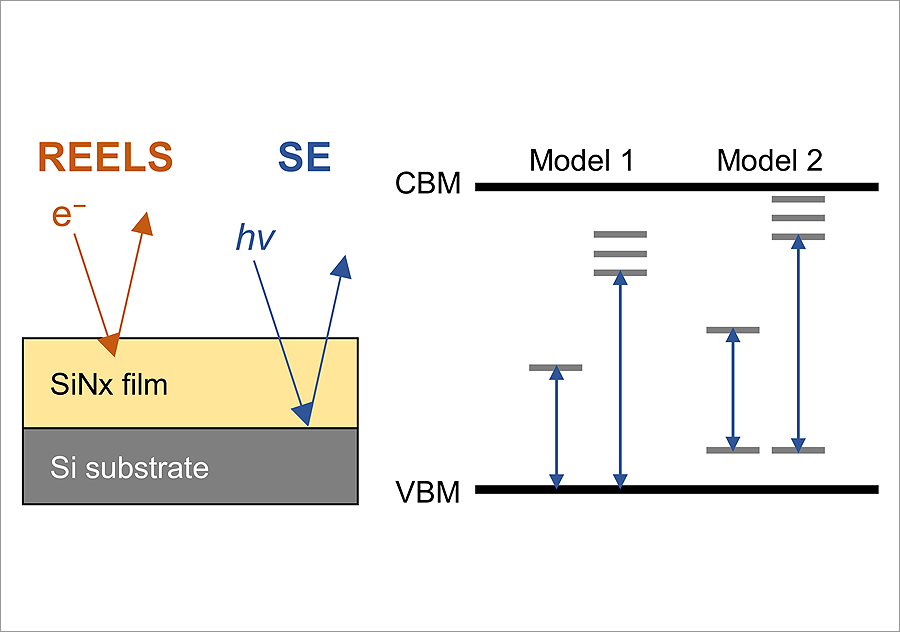
The research team noted that although silicon nitride (SiNx) plays an important role as a charge trap layer in 3D NAND flash memory devices, there is a lack of methods to analyze its operating process. To address this, the research team devised a new analytical method that integrates high-resolution ellipsometry (SE) and electron energy loss spectroscopy (REELS). In this study, the light absorption state occurring in the charge trap layer of a thin silicon nitride film was measured by ellipsometry and the polarization characteristics of the light reflected from the surface were analyzed. In addition, more reliable electronic structure information was obtained by detecting signals from the charge trap layer using electron beam reflection. This technology is an important basic research for the development of next-generation memory semiconductors, and is expected to present a new paradigm for future semiconductor material research.

▲ Professor Jang Young-jun (3rd from left, co-corresponding author), Professor Han Moon-seop (4th from left, co-corresponding author), Professor Choi Eun-jip (right, co-corresponding author)
The results of the study were published on October 24 under the title "Advanced Spectroscopic Methods for probing in-gap defect states in charge trap memory applications" in "Current Applied Physics," an SCI-level international academic journal co-published by the Korean Physical Society and Elsbeer Publishing in the Netherlands.
This study was conducted with the support of the industry-academic research and future element source technology development project of Samsung Electronics Semiconductor Research Institute, and the basic research (group research, mid-sized research) of the Korea Research Foundation. In the research process, the nanofab center and HB solution were in charge of sample analysis.


